Mastering High-Speed Board-to-Board Connector SelectionWhen architectural constraints demand that a system be split across multiple printed circuit boards (PCBs), board-to-board (BTB) connectors serve as the primary electrical and mechanical bridges. Unlike flexible cabling solutions that isolate mechanical stress, a mated pair of BTB connectors establishes a rigid or semi-rigid interfacial connection. This requires hardware engineers to balance precise mechanical tolerances against high-frequency signal integrity requirements. Choosing the right configuration involves evaluating spatial orientation, high-speed differential signaling, and the micro-mechanics of the contact interface.Spatial Topologies and Geometric OrientationsThe physical placement of the PCBs within the enclosure dictates the mating topology. Hardware architectures generally fall into three distinct geometric configurations: Mezzanine (Parallel Stacking): In this topology, two or more PCBs are stacked parallel to each other. The primary selection metric here is the exact stacking height (or profile height), which defines the clearance window between the parallel board faces. This space must accommodate the maximum component heights of surface-mount components (SMDs) populated underneath the upper board.Coplanar (Horizontal Mating): This layout mates two PCBs edge-to-edge on the exact same horizontal plane. It is frequently deployed in linear modular architectures, such as daisy-chained LED strips or modular sensor arrays, where hot-swappable or continuous-trace propagation is needed without adding vertical bulk.Perpendicular (Right-Angle / Orthogonal): Here, one board sits at a 90-degree angle relative to a main motherboard or backplane. This is the structural foundation of enterprise server racks, telecom blade architectures, and daughtercard expansions. It enables massive computing density by vertical stacking, though it introduces complex cooling and mechanical shear challenges.Mechanical Integrity and Tolerance RealitiesRigid BTB interconnects are completely unforgiving when it comes to manufacturing misalignment. Accumulative tolerances across the PCB fabrication, component placement (SMT pick-and-place accuracy), and chassis mounting can result in significant spatial offsets.If a standard, rigid connector pair is forced to mate under these conditions, it induces continuous residual stress on the solder joints, eventually leading to latent solder fatigue or trace cracking under thermal cycling.To mitigate this risk, high-density system designs rely on floating board-to-board connectors. These specialized interconnects feature an internal spring-like mechanical structure that allows the contact matrix to move independently of the soldered base. High-performance floating connectors can absorb misalignments of up to ± 0.5 mm or more in both the X and Y axes, as well as compensate for slight angular tilt during blind-mating assembly sequences.Additionally, engineers must factor in the wiping length—the distance the male pin remains in continuous electrical contact with the female receptacle during the insertion stroke. A longer wiping length ensures a reliable, low-resistance connection even if the connector pair is not fully seated to its nominal depth due to chassis tolerance stack-up.High-Speed Signal Integrity and Power DeliveryModern BTB connectors often sit directly in the path of multi-gigabit serialization protocols, such as PCIe Gen 5/6, USB4, or high-speed networking fabrics. At these frequencies, the connector pin field acts as a transmission line. Any sudden change in geometry introduces an impedance mismatch, causing signal reflections, insertion loss, and inter-symbol interference (ISI).To maintain a clean 85-ohm or 100-ohm differential impedance profile, advanced BTB connectors utilize specialized pin geometries and internal grounding shields. By wrapping signal pairs with dedicated ground blades, the connector minimizes crosstalk between adjacent lines. Pin-out design is equally critical; engineers must interleave ground pins around differential signal pairs (a common G-S-S-G pattern) to provide a tight, controlled return path for high-frequency currents.Finally, managing the physical real estate means optimizing the pin pitch. While ultra-fine pitches (0.4 mm to 0.5 mm) maximize the signal density per square millimeter, they severely limit the maximum current carrying capacity per pin, often capping out at less than 0.5 A per contact.For architectures requiring substantial power delivery alongside high-speed data, hybrid board-to-board connectors are the ideal choice. These configurations integrate dedicated, heavy-duty power blades (capable of handling up to 3 A to 10 A each) on the outer flanks of the connector housing, leaving the center pitch fully optimized for sensitive, low-voltage differential signaling.
Mastering High-Speed Board-to-Board Connector Selection

Related Articles
More in Board-To-Board →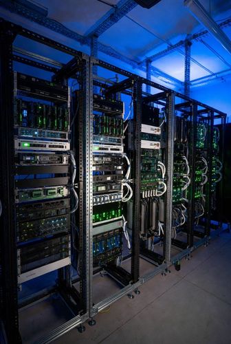
Board-To-Board
Floating and Self-Aligning Board-to-Board Connectors for High-Density Systems
Mating multiple parallel or perpendicular PCBs can induce solder joint strain due to tolerance stack-up. Learn how floating Board-to-Board connectors absorb mechanical misalignment.
24 JUL 2026Read →
Board-To-Board
Board-to-Board Mezzanine vs. Cable-to-Board Interconnects: Architectural Trade-Offs in Hardware Design
Choosing between mezzanine board-to-board connectors and cable-to-board assemblies impacts stack height, thermal dissipation, and signal paths. Here is a practical engineering guide.
24 JUL 2026Read →
Board-To-Board
Engineering High-Speed Board-to-Board Connector Interfaces for Multi-Gigabit Signal Integrity
A high-speed board-to-board connector is a fundamentally different class of hardware than a standard low-frequency part — every element of its physical architecture is precision-modeled as a continuous transmission line.
20 JUL 2026Read →
Board-To-Board
Blind-Mate Backplane Connectors: Guide Pins, Floating Housings, and Insertion Force Management
A technician sliding a 40-pound blade into a rack slot can't see the connector at the moment it matters most. Blind-mate backplane connectors solve this with guide pins, floating housings, and carefully managed insertion force.
20 JUL 2026Read →