Introduction: The Physics of High-Frequency Pipelines
As data rates in enterprise datacenters, AI training clusters, and telecommunication nodes surge past 56 Gbps and 112 Gbps per channel using advanced modulation schemes like PAM4 (Pulse Amplitude Modulation 4-Level), the traditional perception of a connector changes. At these extreme frequencies, a board-to-board connector can no longer be modeled as a simple, benign metal path. It behaves as a highly complex waveguide.
Every geometric shift, pin transition, and plastic dielectric boundary within the connector introduces major potential failure points. Designing and specifying high-speed board-to-board connectors requires managing high-frequency physics, minimizing signal loss, and mastering electromagnetic interference (EMI) containment.
Part 1: The Core Metrics of Signal Integrity
When evaluating high-speed interconnect arrays, signal integrity (SI) engineers focus heavily on a set of frequency-dependent performance parameters, typically visualized via Scattering Parameters (S-Parameters).
1. Differential Impedance Control
To prevent catastrophic signal reflections, the entire interconnect path must match the system's characteristic differential impedance—typically 85 Ohm for PCIe-based architectures or 100 Ohm for standard Ethernet networks. Connector manufacturers achieve this by precisely tuning the cross-sectional geometry of the stamping pins and controlling the spacing between the signal contacts and adjacent ground shields. Any sudden variation in this ratio creates an impedance drop or spike, degrading the system's return loss.
2. Insertion Loss (S21)
Insertion loss measures the total attenuation of signal power as it travels through the mated connector interface. At high frequencies, insertion loss is driven both by skin effect losses within the copper metal and dielectric absorption within the surrounding plastic housing. High-speed connectors utilize low-loss, specialized polymer blends to keep insertion loss minimal across target operating frequencies.
3. Crosstalk Mitigation (S31, S41)
Crosstalk occurs when the intense electromagnetic field radiating from an active signal pin couples into an adjacent victim pin. This is categorized as Near-End Crosstalk (NEXT) or Far-End Crosstalk (FEXT). Left unchecked, crosstalk destroys the delicate voltage eyes of high-speed signals, rendering data unreadable.
Part 2: Advanced Structural Shielding — The Open-Pin Field Evolution
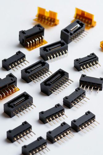
To achieve clean data transmission at multi-gigabit speeds, modern high-speed board-to-board connectors utilize an optimized open-pin field array configuration with embedded ground shields.
Instead of relying on basic, unprotected rows of pins, high-speed connector systems embed internal ground blades or allow engineers to surround every differential signal pair with dedicated ground pins. This layout creates an internal Faraday cage around each signal pair, completely suppressing multi-line crosstalk and allowing high-frequency differential pairs to be routed directly adjacent to one another without sacrificing signal fidelity.
Part 3: The Critical Footprint — Optimizing the PCB Breakout Region
A connector can feature outstanding internal specifications, but its ultimate real-world performance is entirely bounded by how well it integrates with the PCB. The region where the connector pins enter the PCB layout is known as the Breakout Region (BOR) or Footprint.
Engineers must optimize the BOR via advanced layout strategies:
- Anti-Pads: Removing the internal ground and power planes directly beneath the connector's SMT pads or through-hole vias to minimize parasitic capacitance, which would otherwise drop the localized impedance below acceptable thresholds.
- Via Stub Drilling: For through-hole or press-fit connectors, any remaining portion of the copper via barrel extending past the active routing layer acts as a signal-destroying stub. High-speed systems mandate back-drilling to physically drill out these excess via stubs, preserving high-frequency signal clarity.
Performance Takeaway: Waveguide Compliance
At multi-gigabit data scales, high-speed board-to-board connectors act as primary gatekeepers of system throughput. Successfully implementing these high-frequency interfaces requires an end-to-end understanding of impedance tracking, insertion loss limits, and advanced Faraday shielding architectures. By tightly pairing low-loss connector matrices with optimized PCB breakout footprints, engineers ensure that high-frequency pipelines maintain rock-solid data integrity.