The Challenge of Mechanical Tolerance Stack-Up in Multi-Board Systems
Modern industrial automation, automotive domain controllers, and high-density networking hardware frequently rely on modular architectures where multiple daughter cards connect to a single backplane or motherboard. Mating two rigid PCBs using a single board-to-board connector is straightforward. However, when a design calls for mating two boards using multiple parallel connectors simultaneously, or when boards are housed inside rigid die-cast enclosures, mechanical alignment challenges multiply.
Every manufacturing step introduces dimensional variations: PCB fabrication tolerances, drill hole placement errors, SMT component placement offsets, and enclosure machining tolerances. When these individual variations combine—a phenomenon known as mechanical tolerance stack-up—the physical position of two mating connector headers can deviate by several tenths of a millimeter. Forcing rigid connectors into alignment during assembly applies severe mechanical shear stress to the surface-mount solder joints, resulting in cracked pads, micro-fractured solder balls, or cracked connector housings.
How Floating Connector Architectures Work
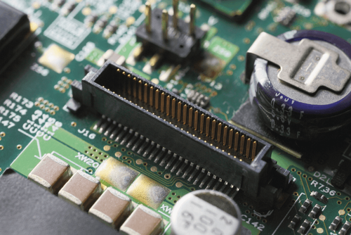
To resolve alignment errors without requiring ultra-tight (and costly) enclosure manufacturing tolerances, connector manufacturers developed floating Board-to-Board (B2B) connectors. Unlike standard rigid SMT headers, floating connectors incorporate an internal spring-beam structure within their plastic housing.
This flexible contact spring allows the mating interface of the connector to float along the X, Y, and Z axes relative to the fixed SMT solder pads anchored to the PCB. Commercial floating connectors typically provide movement tolerances of ±0.5 mm to ±1.0 mm in both the X and Y directions, along with a Z-axis absorption range to accommodate board distance variations. As the male header enters the female receptacle, internal spring contacts flex smoothly, absorbing mechanical misalignments without transferring bending forces to the underlying solder joints.
Self-Aligning Design Features for Automated Assembly
In high-volume automated manufacturing, operators or robotic pick-and-place arms must mate boards quickly without damaging pins. Self-aligning connector housings feature wide chamfered entry funnels (lead-in guides) around the outer perimeter of the connector shell.
These mechanical entry guides pick up the mating connector even if it approaches off-center by up to 1.5 mm or at an angle of several degrees. As the boards press together, the lead-in ramps glide the floating contact block into alignment, clicking into full engagement. This self-correcting behavior eliminates manual pin alignment steps, reduces assembly time, and prevents bent contact terminals on production lines.
High-Speed Signal Integrity in Floating Contacts
Historically, adding flexible internal spring beams to a connector compromised signal integrity, as long unshielded contact springs introduced parasitic inductance and impedance discontinuities. Modern floating B2B connectors overcome this through optimized contact geometry and integrated ground shielding.
Advanced floating connectors feature dual-contact spring beams that maintain continuous electrical contact even under shock and vibration. Tightly controlled contact impedance supports high-speed data transmission rates up to 8 Gbps, 16 Gbps, or PCIe Gen 4 speeds. This enables system designers to route high-speed buses across modular boards while retaining complete immunity to mechanical tolerance stack-up and thermal expansion strain.
System Integration Guidelines
When integrating floating board-to-board connectors into multi-board products, designers should apply key layout principles:
- Combine Rigid and Floating Connectors Correctly: When joining two boards with multiple connectors, designate one connector as the fixed primary reference point and make all remaining connectors floating types to absorb positional variance.
- Verify SMT Pad Anchoring: Ensure surface-mount solder tabs (hold-downs) feature generous copper pad areas to anchor the fixed base of the floating housing securely to the PCB.
- Account for Clearances: Maintain sufficient physical spacing around the floating connector housing on the PCB layout to allow the floating mechanism to move freely throughout its full tolerance range without contacting adjacent components.