The Dual Demands of Power Delivery and Shrinking Space
Modern handheld devices, robotics, smart home products, and medical instruments face a dual engineering challenge: internal circuit boards continue to shrink, yet power requirements keep rising. High-performance processors, bright displays, and fast-charging battery systems demand continuous currents ranging from 3 A to 10 A or more, while simultaneous control systems require dozens of fine-pitch signal lines for high-speed data, sensor telemetry, and system management.
Historically, hardware designers allocated separate connectors for power and data—a dedicated high-current terminal block alongside a fine-pitch signal connector. In ultra-compact enclosures, however, dedicated power connectors consume unacceptably large PCB areas. To conserve board space, system designers increasingly adopt hybrid power and signal connectors that integrate high-current contacts and fine-pitch signal lines within a single compact housing.
Architecture of Hybrid Connectors: Power Blades and Signal Arrays
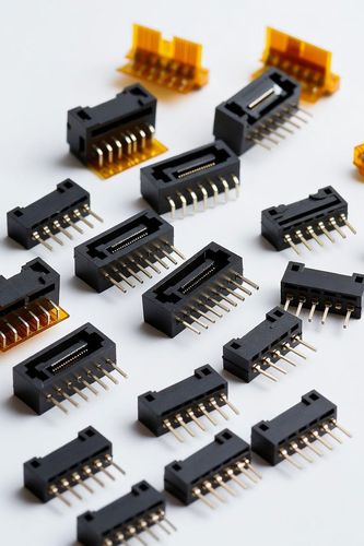
Hybrid connectors achieve miniaturization by utilizing specialized dual-geometry contact structures. Instead of using identical uniform pins across the entire connector array, hybrid housings combine two distinct contact types:
- Power Blades/Pins: Heavy-duty, low-resistance copper alloy contacts positioned at the outer ends of the connector housing. These wide contact blades feature thick cross-sectional areas capable of carrying 3 A to 10 A per pin continuously with minimal resistive heating.
- Signal Pin Arrays: Fine-pitch micro-contacts (0.35 mm to 0.5 mm pitch) clustered in the central region of the housing. These delicate pins transmit high-speed data, I2C/SPI control buses, and sensor signals where current requirements remain under 0.5 A per line.
By placing heavy power blades at the housing ends, manufacturers also leverage them as mechanical anchor tabs. These robust power terminals absorb insertion forces and cable strain, protecting the delicate central signal pins from mechanical deformation.
Thermal Management and Current Derating Rules
The primary engineering constraint in hybrid power and signal design is thermal rise. Passing high currents through compact connector contacts generates Joule heating (I²R loss). If internal connector temperatures rise too high, plastic housings can soften, spring contact forces drop due to stress relaxation, and insulation resistance degrades.
To maintain safe operating conditions, engineers must apply thermal derating rules:
- Calculate Ambient Temperature Spans: Connector current ratings are typically specified at an ambient temperature of 20°C. In sealed electronics where internal temperatures reach 60°C or 80°C, the maximum allowable current must be derated according to manufacturer thermal curves.
- Parallel Signal Pins Correctly: If dedicated power blades are unavailable, designers sometimes route power across multiple parallel signal pins. Apply a 20% to 30% current derating factor when ganging signal pins together for power delivery.
- Optimize Copper Pour Area: Connect wide copper planes directly to the SMT pads of the power blades. These copper pours act as localized thermal heat sinks, conducting heat away from the connector pins and out through the PCB ground planes.
Preventing Crosstalk and Noise Coupling in Hybrid Layouts
Placing high-current power lines directly adjacent to sensitive signal traces inside a single connector housing introduces electromagnetic interference (EMI) risks. Rapid load switching on power rails can induce inductive voltage spikes or capacitive noise into adjacent high-impedance data lines.
To preserve signal integrity in hybrid interconnects:
- Incorporate Isolation Shield Pins: Assign ground reference pins between power blades and sensitive high-speed signal pairs to act as an internal shield against magnetic field coupling.
- Filter Power Lines at the Connector Entry: Place ceramic decoupling capacitors (0.1 μF and 10 μF) immediately adjacent to the connector power pins to bypass high-frequency switching noise directly to ground before it radiates across the board.
- Segregate PCB Trace Routing: Keep power traces on separate copper layers or maintain generous physical spacing from high-speed differential signal routes as they exit the hybrid connector footprint.