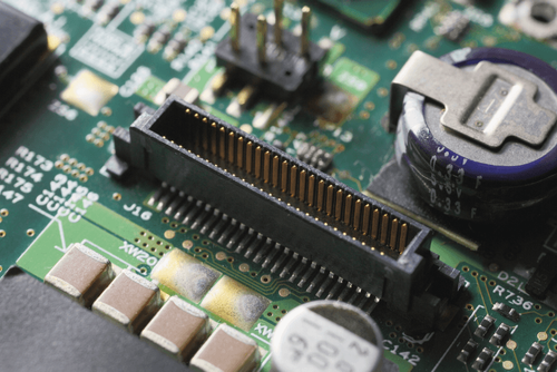
As electronic devices shrink in physical footprint while their data processing capabilities scale exponentially, internal PCB architecture has had to adapt. Traditional internal wiring is rapidly being replaced by dense, multi-board stacked configurations connected through high-speed board-to-board connectors — components engineered specifically to pass multi-gigabit data streams between coplanar, perpendicular, or parallel circuit boards. Achieving clean transmission at frequencies exceeding 28 GHz requires a genuinely different design discipline than a standard board-to-board part, built around contact geometry, impedance matching, and adherence to real industry standards.
What Actually Separates a High-Speed Connector From a Standard One
Standard board-to-board connectors are designed for low-frequency control signals or power routing, where cost and basic mechanical durability are the priorities. A high-speed variant is a categorically different piece of hardware — every element of its internal architecture is precision-modeled to function as a continuous transmission line, not just a mechanical bridge. Three features define this class of part:
Integral ground planes — built-in metallic ground plates positioned between rows of signal pins, providing low-impedance return paths and actively suppressing crosstalk between adjacent differential pairs, rather than relying on pin spacing alone to keep signals isolated.
Low-profile contact geometry — advanced contact structures that minimize the physical length of the electrical path itself, directly reducing propagation delay and parasitic capacitance, both of which matter more at each successive generation of higher data rates.
Variable stack heights without electrical compromise — manufacturers now offer mezzanine connectors across a range of stack heights while holding high-frequency performance constant, rather than forcing a tradeoff between mechanical clearance and signal integrity the way earlier connector generations often did.
Intermateability: Why Cross-Vendor Compatibility Is a Real Engineering Question
In sourcing and design, a connector is described as intermateable if it can physically mate with, and perform identically alongside, a connector manufactured by a competing vendor. In the high-speed connector world specifically, genuine cross-vendor compatibility is harder to guarantee than it sounds, because proprietary pin geometries, vendor-specific patents, and tight manufacturing tolerances can all quietly break what looks like a drop-in replacement on paper.
Industry standards exist specifically to solve this: PCIe, the Open Compute Project (OCP), and COM Express all mandate open architectures precisely so that intermateability can be verified rather than assumed. When selecting a high-speed connector, engineers need to confirm that a proposed second-source part is genuinely intermateable across footprint, wipe length, spatial clearance, and signal integrity performance — not just physically compatible on a datasheet dimension drawing. Verified intermateability is also a direct supply chain risk mitigation, since it protects a design from being trapped on a single-source component if that vendor hits a production delay of the kind covered in our piece on transceiver and backplane lead-time bifurcation.
PCB Layout: Where the Connector's Design Meets the Board's
Even a perfectly engineered high-speed connector fails to deliver its rated performance without matching discipline on the surrounding PCB layout. When a differential trace transitions from the horizontal plane of the board into the vertical plane of the connector, it crosses a real physical discontinuity — and how that transition is handled determines whether the connector's rated performance is actually achieved in practice.
Two techniques matter most. Anti-pad optimization — precisely modeling the clearances cut into the copper ground planes directly beneath the connector's pins — minimizes the added capacitance those pads would otherwise introduce at the transition. Backdrilling — removing the unused copper stub left behind when a via only needs to route a signal partway through a multi-layer board — eliminates what would otherwise function as a small resonant antenna, distorting the high-frequency waveform passing nearby. This same backdrilling discipline governs board-to-board signal integrity at rates well beyond PCIe Gen 6, and is covered in more depth in our guide to ultra-low profile PCIe Gen 7 connector design, where via stub elimination becomes even more critical at a 64 GHz Nyquist frequency.
Combining precision-engineered connector hardware with this kind of disciplined PCB layout is what actually delivers flawless data rates across complex, multi-board embedded systems — and it's the connector-and-layout half of the broader architectural picture covered in our server backplane architecture guide.