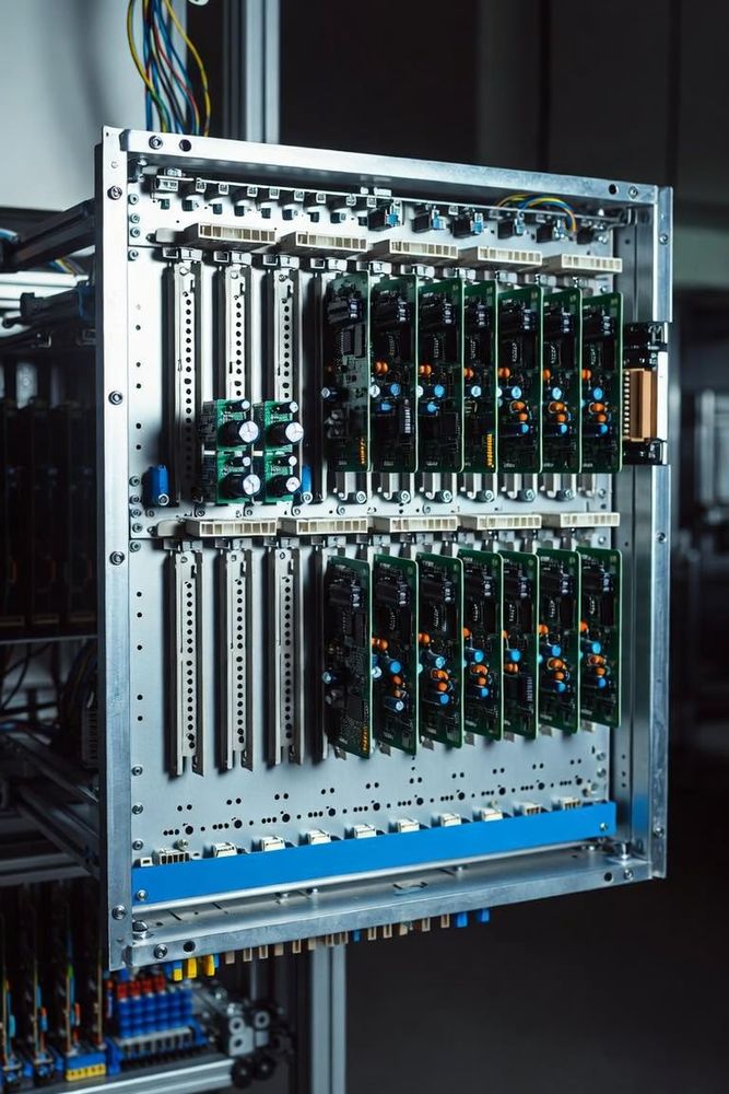
The Backplane as a System Backbone
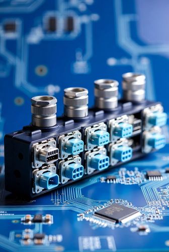
In enterprise data centers, blade servers, and high-performance telecom routing racks, throughput is gated by how effectively data can transition across the system backbone. High-speed backplane connectors act as the primary structural and electrical intersection, linking modular daughter cards to a centralized system management board. Operating at transmission speeds that push past 56 Gbps and 112 Gbps per channel, these massive interconnect matrices must be co-engineered as a single continuous wave-guiding system to prevent catastrophic signal degradation.
Orthogonal Direct Connector Systems
Traditional backplane architectures rely on a passive midplane board where daughter cards plug in from the front and line cards plug in from the back. The signals are routed through complex trace paths within the midplane layer stackup. However, as data rates scale into the multi-gigabit regime, the dielectric losses and skin effect attenuation of long PCB traces quickly deplete the signal's energy.
To overcome this structural barrier, high-speed architectures utilize orthogonal direct connector systems. In this layout, the front daughter cards are oriented vertically, while the rear cards are oriented horizontally. The high-speed connectors mate directly through precision slots in a thin midplane, completely eliminating the need for signal routing traces inside the midplane core. This direct-connect method slashes the signal path length to the thickness of a single connector block, drastically lowering insertion loss and crosstalk.
Via Stub Backdrilling
The physical mounting footprint of a backplane connector uses Plated Through-Hole (PTH) press-fit pins. When a signal transitions from a horizontal PCB trace down into a vertical press-fit pin, it encounters a metallic via column. The portion of the via that extends past the active signal layer acts as an open-circuited transmission line stub. This stub introduces massive capacitive loading and creates signal reflections that can entirely cancel out specific operating frequencies.
To fix this, backplane designers implement backdrilling (automated depth control drilling). A secondary drill bits out the unused copper via columns, eliminating the stubs and restoring a clean, uniform impedance profile across the vertical channel transition.
Internal Shielding and Impedance Control
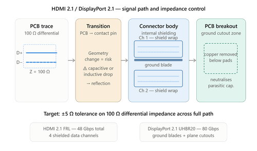
Maintaining absolute impedance uniformity requires precise control over the connector's internal lead-frame geometry. The metal contacts inside high-speed backplane housings are stamped with continuous wide-ground planes that tightly shield every individual differential signal pair. The spatial gap between the dual signal pins and their surrounding ground shields is finely tuned to hit a target differential impedance—typically 85 Ohm for PCIe networks or 100 Ohm for Ethernet structures.
Co-Engineering the Connector and the Board
By managing internal shielding geometries, optimizing the physical PCB via breakout region, and eliminating unused via stubs, backplane connectors allow clean data transport across the core of enterprise server frameworks.