Introduction: Moving Beyond Two-Board Architectures
While standard mezzanine connectors are perfectly optimized for connecting a single daughtercard to a primary motherboard, many complex industrial, aerospace, and embedded processing applications require a far more scalable expansion path. When a system must dynamically adapt to add extra sensor cards, variable memory blocks, or modular power stages, a simple two-board layout falls short.
This is where stackable board-to-board connectors excel. Utilizing specialized pass-through pin architectures, these components allow multiple PCBs to be stacked directly on top of one another like building blocks, sharing a single unified system-wide electrical bus that runs vertically through the entire stack.
Part 1: The Anatomy of Pass-Through Pin Mechanics
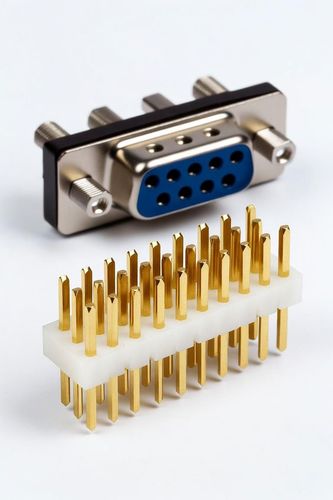
The core innovation behind stackable interconnects is the pass-through (or stackable) header. Unlike standard headers that terminate abruptly at the PCB surface, stackable pins are extended, dual-sided elements that exit both the top and bottom faces of the connector housing.
A single pin acts simultaneously as the solder interface for the middle board, the male plug for the board above it, and the female socket receiver for the board below it. Designing these contacts requires meticulous length calculations:
- Mating Length: The upper portion of the pin must extend far enough to fully engage the wiping mechanism of the upper board's receptacle.
- Tail Length: The lower tail must clear the thickness of the local PCB substrate with enough exposed metal to form a clean, IPC-A-610 compliant solder fillet, while still plunging securely into the underlying connector receptacle.
Part 2: Legacy and Modern Architectural Standards
The PC/104 and PC/104-Plus Paradigm
Traditional PC/104 modules utilize a 104-pin, 2.54 mm (0.100 inch) pitch stackable bus structure. The modules are stacked mechanically using threaded standoffs, while the connectors form a self-stacking ISA expansion bus.
As bus speeds advanced, the standard evolved into PC/104-Plus, which integrated a secondary, fine-pitch (2.0 mm) stackable connector to support high-speed PCI bus traffic alongside the legacy ISA signals, proving that multi-tier architecture could scale alongside processing performance.
Part 3: Signal Integrity and Bus Loading in Multi-Tier Stacks
Cumulative Stub Effects
In a multi-tier stack, a signal originating on the base motherboard traveling to the topmost card must pass through every intermediate connector. Each unused pass-through contact hanging below or extending above the active circuit acts as an unterminated electrical stub. These stubs cause severe impedance discontinuities. When high-speed signal edges hit an unterminated stub, a portion of the wave energy reflects backward down the line, distorting the primary signal and causing data corruption or bit errors.
Capacitive Bus Loading
Every added tier introduces more contact metal and another localized solder joint, multiplying the overall parasitic capacitance of the line. This cumulative capacitive load slows down signal rise and fall times, restricting the maximum operational frequency of shared stackable buses. While power distribution lines can be stacked across 6 to 10 layers smoothly, high-speed data buses across stackable configurations are typically limited to 3 or 4 layers before active buffers or redrivers become mandatory.
System-Level Takeaway: Balancing Modularity and Bandwidth
Stackable board-to-board connectors provide a flexible framework for expanding embedded and industrial computing systems. Successfully deploying a multi-tier design requires moving beyond raw mechanical stacking to analyze the underlying electrical impacts of pass-through pins. By calculating tail tolerances, managing capacitive bus loads, and mitigating the wave reflections born from unterminated stubs, engineers can build robust, highly scalable stacks that maximize processing potential in limited volumes.