Introduction: The PCIe Scaling Challenge
The PCI Express (PCIe) bus is the central nervous system of high-performance computing, channeling massive data streams between the central processing unit, graphics processing units, and ultra-fast NVMe storage arrays. PCIe Gen 5 operates at 32 GT/s per lane, while PCIe Gen 6 doubles that capacity to 64 GT/s per lane. For connector engineers, this rapid scaling requires redesigning the classic card-edge interface to handle frequencies that push deep into the microwave spectrum.
The Shift from THT to SMT
The fundamental challenge of PCIe connector evolution is maintaining backward compatibility with the classic vertical card-edge form-factor while completely overhauling the underlying electrical performance. Up through PCIe Gen 4, standard through-hole press-fit connectors were sufficient. However, at Gen 5 and Gen 6 frequencies, the long vertical lead-frames and solder pins of traditional through-hole connectors act as massive inductive bottlenecks.
To hit strict signal integrity baselines, the industry shifted to Surface Mount Technology (SMT) and hybrid land-grid/surface-mount card-edge connectors. By resting directly on the top copper layer of the PCB, SMT PCIe connectors eliminate vertical pin extensions, drastically cutting parasitic inductance and reducing channel insertion loss.
Short-Beam Contact Profiles for Gen 6
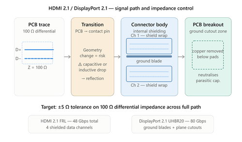
At PCIe Gen 6 speeds, the physical geometry of the connector's internal gold-plated contacts can cause major issues. When the add-in card is slid into the connector slot, the card's gold fingers slide past the connector's spring beams. The unused metallic overhang of the spring contact creates a tiny open stub. At 64 GT/s, this stub creates a localized capacitive discontinuity that triggers signal reflections and severe phase jitter.
To combat this, Gen 6 compliant card-edge connectors deploy specialized "short-beam" contact profiles that minimize overhang, along with optimized plastic housings that feature tuned air pockets to keep the local differential impedance locked at 85 Ohm.
PAM4 Crosstalk Sensitivity
PCIe Gen 6 introduces a major shift in signaling architecture, migrating from traditional NRZ binary signaling to multi-level PAM4. Because PAM4 packs more data into the same time slice by using four distinct voltage levels instead of two, the voltage steps between states are dramatically smaller. This makes PCIe Gen 6 channels exceptionally sensitive to near-end crosstalk (NEXT) and far-end crosstalk (FEXT) within the connector pin field.
Next-generation PCIe layouts require isolating high-speed transmit and receive lanes with alternating ground pins, coupled with tight manufacturing tolerances to ensure absolute coplanarity across the entire multi-position card-edge grid.
Co-Design at the Speed of Silicon
PCIe Gen 5 and Gen 6 connectors demand a complete co-design approach between the connector manufacturer, the PCB layout engineer, and the system architect. Surface mount migration, short-beam contacts, and tight crosstalk isolation are no longer optional refinements — they are mandatory prerequisites for reaching full bandwidth potential.