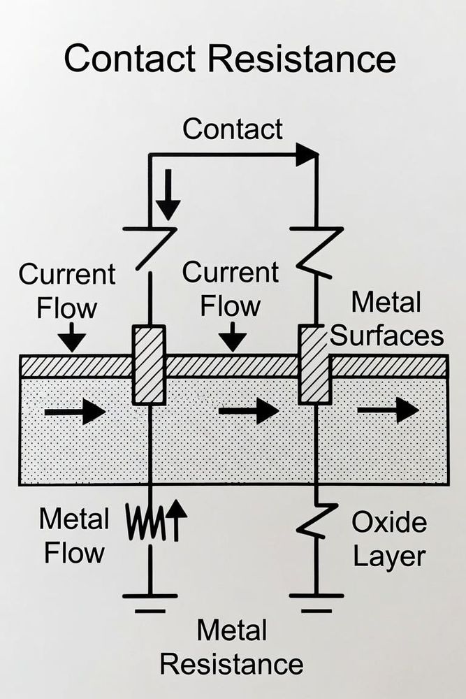
What is Connector Contact Resistance?
In an ideal circuit, a mated connector pair acts as a continuous, zero-resistance metallic conductor. In reality, every physical interface introduces a small amount of electrical resistance across the mating junction, known as contact resistance. Measured in milliohms (mΩ), contact resistance typically ranges from under 5mΩ for high-power interfaces to 20mΩ–50mΩ for fine-pitch signal interconnects.
While a few milliohms may seem negligible, in high-current power distribution networks (PDNs) or sensitive ultra-low-voltage analog interfaces, unmanaged contact resistance leads to severe thermal dissipation (I²R losses) and signal integrity degradation.
The Anatomy of Contact Resistance
Total connector resistance across a mated terminal pair is the sum of three distinct physical components:
1. Bulk Resistance
Bulk resistance is the intrinsic electrical resistance of the solid metal terminal bodies themselves, determined by the resistivity of the metal alloy (brass, phosphor bronze, or beryllium copper), cross-sectional area, and overall physical length of the pins.
2. Constriction Resistance
On a microscopic level, even highly polished metal contact surfaces are rough, featuring microscopic peaks and valleys called asperities. When two contacts touch, physical contact occurs only at these microscopic high points (a-spots). Because electrical current is forced to constrict and flow through these tiny micro-junctions rather than the full cross-sectional area of the pin, current density spikes, creating constriction resistance.
3. Film Resistance
Film resistance is caused by thin, non-metallic surface layers—such as oxides, sulfides, organic contaminants, or moisture films—trapped between the touching contact asperities. If the mechanical wiping action of the contact cannot breach these insulating films, film resistance increases dramatically, sometimes leading to an open circuit.
Key Design Factors Influencing Contact Resistance
Hardware engineers can control contact resistance through component specification and layout decisions.
Normal Force and Contact Geometry
Increasing the mechanical normal force applied by the female spring beam compresses microscopic asperities, expanding the effective contact surface area and lowering constriction resistance. However, higher normal forces increase insertion effort and accelerate plating wear over multiple mating cycles.
Mechanical Wiping Action
High-reliability connectors are engineered with a mechanical "wipe" distance—a small sliding motion between the male pin and female beam during final insertion. This sliding motion physically shears through surface oxide films and pushes away micro-contaminants, establishing clean metal-to-metal contact asperities.
Thermal Effects and Temperature Rise
As current passes through contact resistance, power is dissipated as localized heat. This local heating increases the electrical resistivity of the metal contacts, which in turn elevates resistance further. If unmanaged, this thermal feedback loop can soften spring materials, lower normal force, and eventually cause thermal runaway or melted housing plastic.
Engineering Best Practices for Low Resistance Layouts
To minimize contact resistance risks in your PCB design:
- Specify Low-Resistivity Plating: Gold and silver plating offer superior conductivity and freedom from oxide films compared to tin, maintaining low contact resistance across wide temperature ranges.
- Paralleling Multiple Pins for Power: When routing power rails through fine-pitch connectors, split the high current across multiple parallel pins. This reduces effective contact resistance through parallel resistance laws and spreads thermal dissipation across a larger copper surface area on the PCB.
- Account for Environmental Ageing: Always evaluate a connector's end-of-life contact resistance spec rather than just its fresh, out-of-the-box rating. Dust, humidity, thermal cycling, and chemical exposure cause contact resistance to creep upward over time.